Software
WinPC-Nc
KiCad
Arduino IDE
For this week i made a board that has switches that has to act like Endtops.When a button is pushed it has to give a sign that a process is stopped.Further i will give a explantion how the board is designed,how the board is made and how it is programmed.
Group assignment
Read about the group assignmentInvidual assignment
The hello button board i redesigned
KiCad schematic design
First you have to install the library of the academy in the KiCad library to get the component you need to make the board designs.The library you can get on this link https://gitlab.cba.mit.edu/pub/libraries.
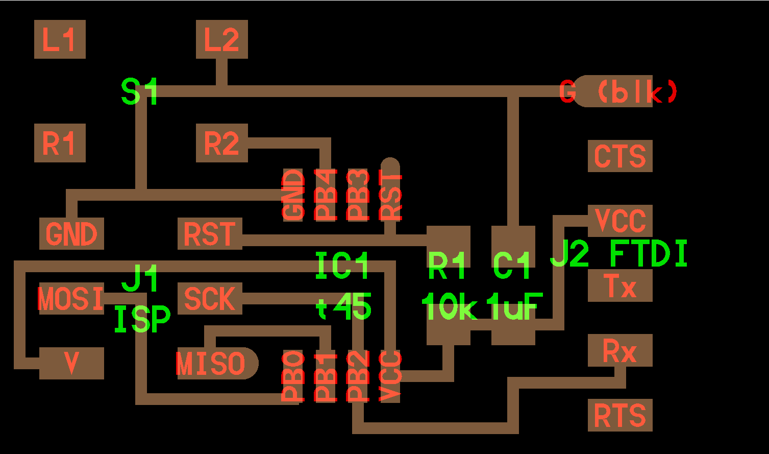
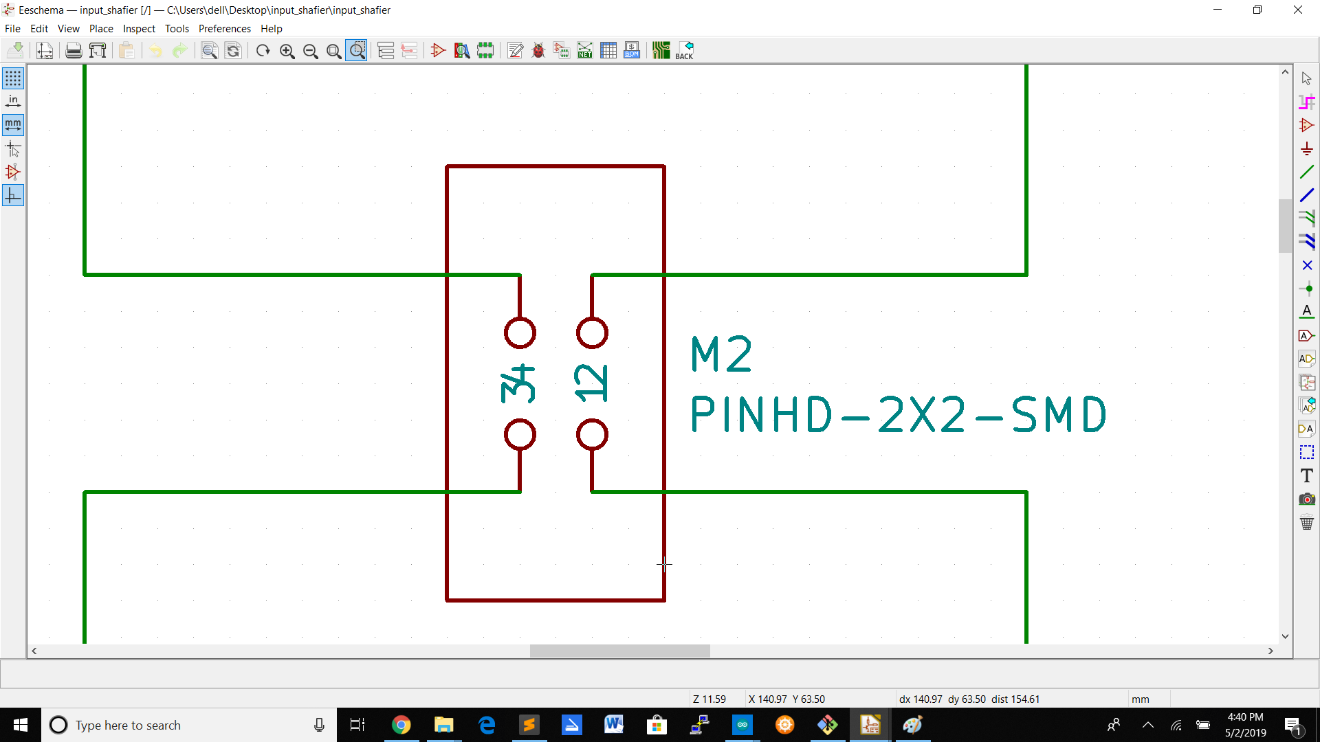
I made my schematic design in KiCad and this design has :
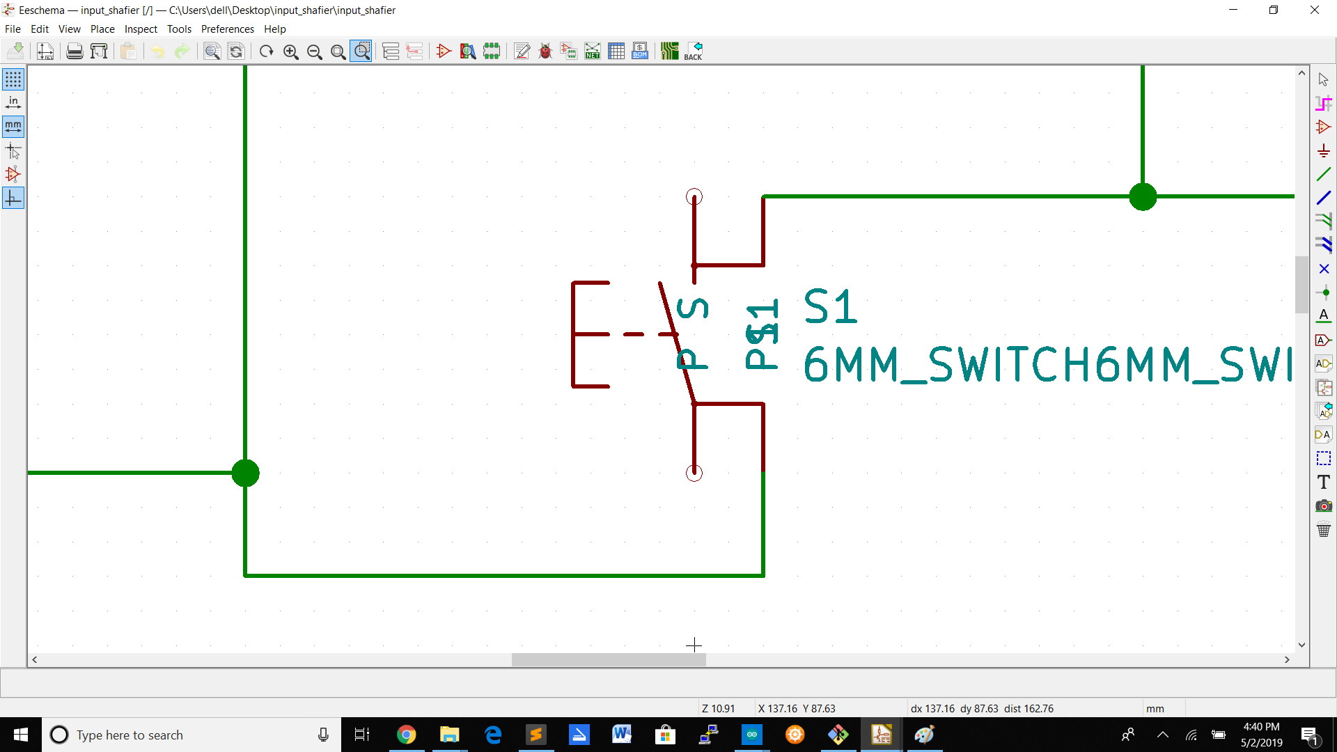
2* Switches
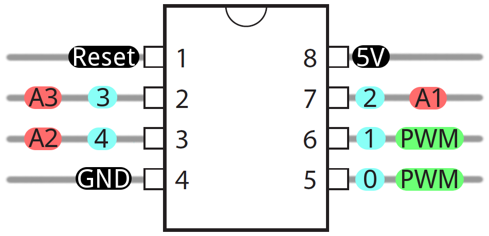
1*ATtiny 45
1*AvrIsp
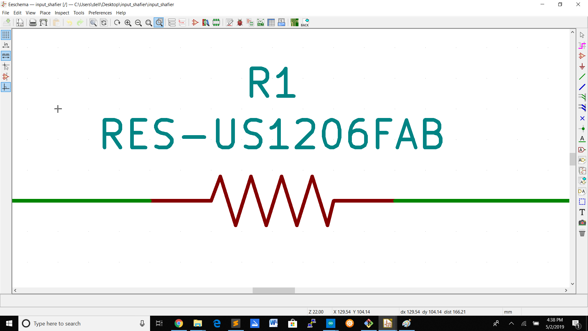
1*10K resistor
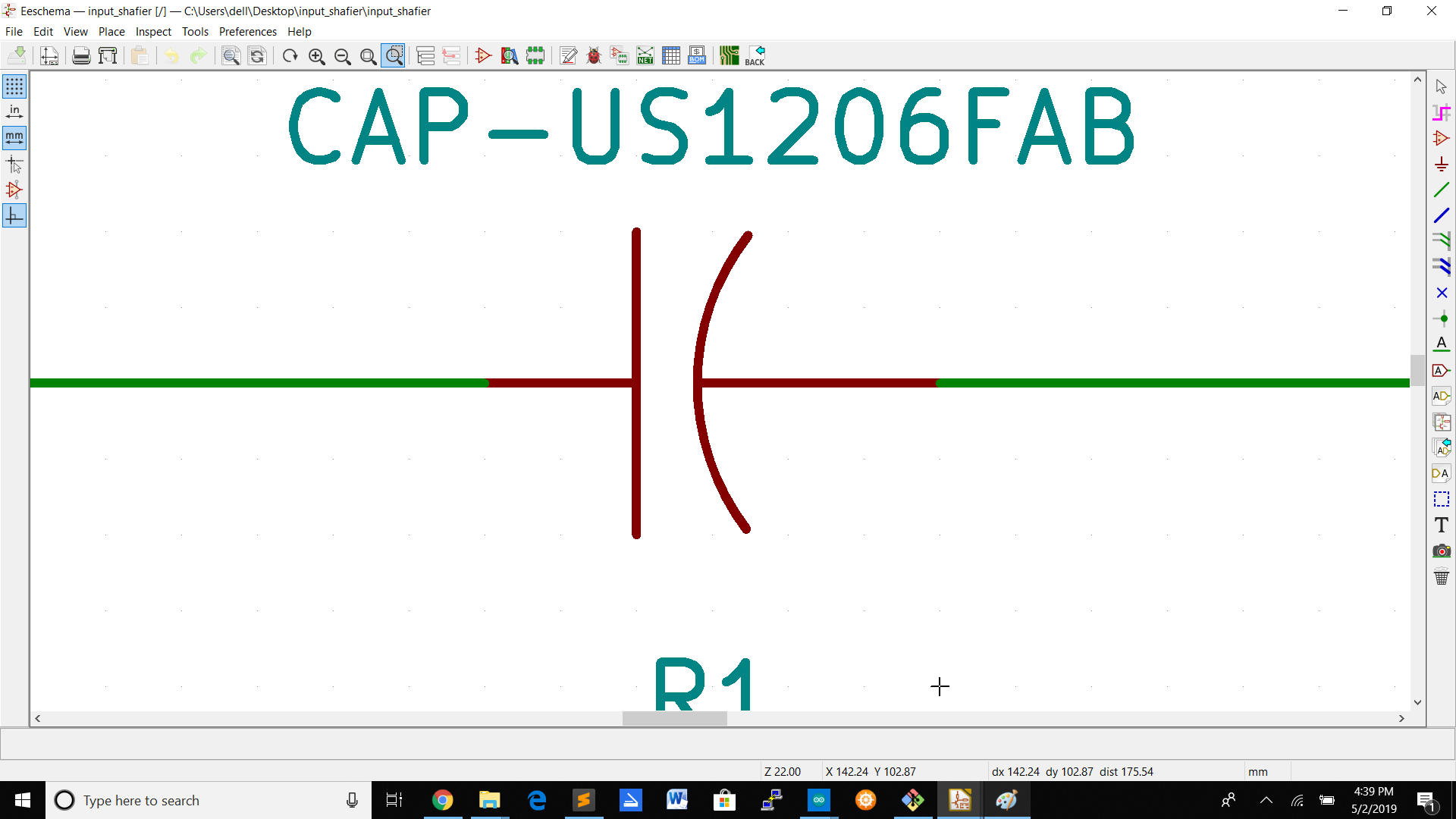
1*1uf capacitor
1*2x2pinheader
1*6pinheader
1*FTDI-SMD pinheader
You have to select the components you are going to need/use for your board.Beneath you see the components i need to make my board.
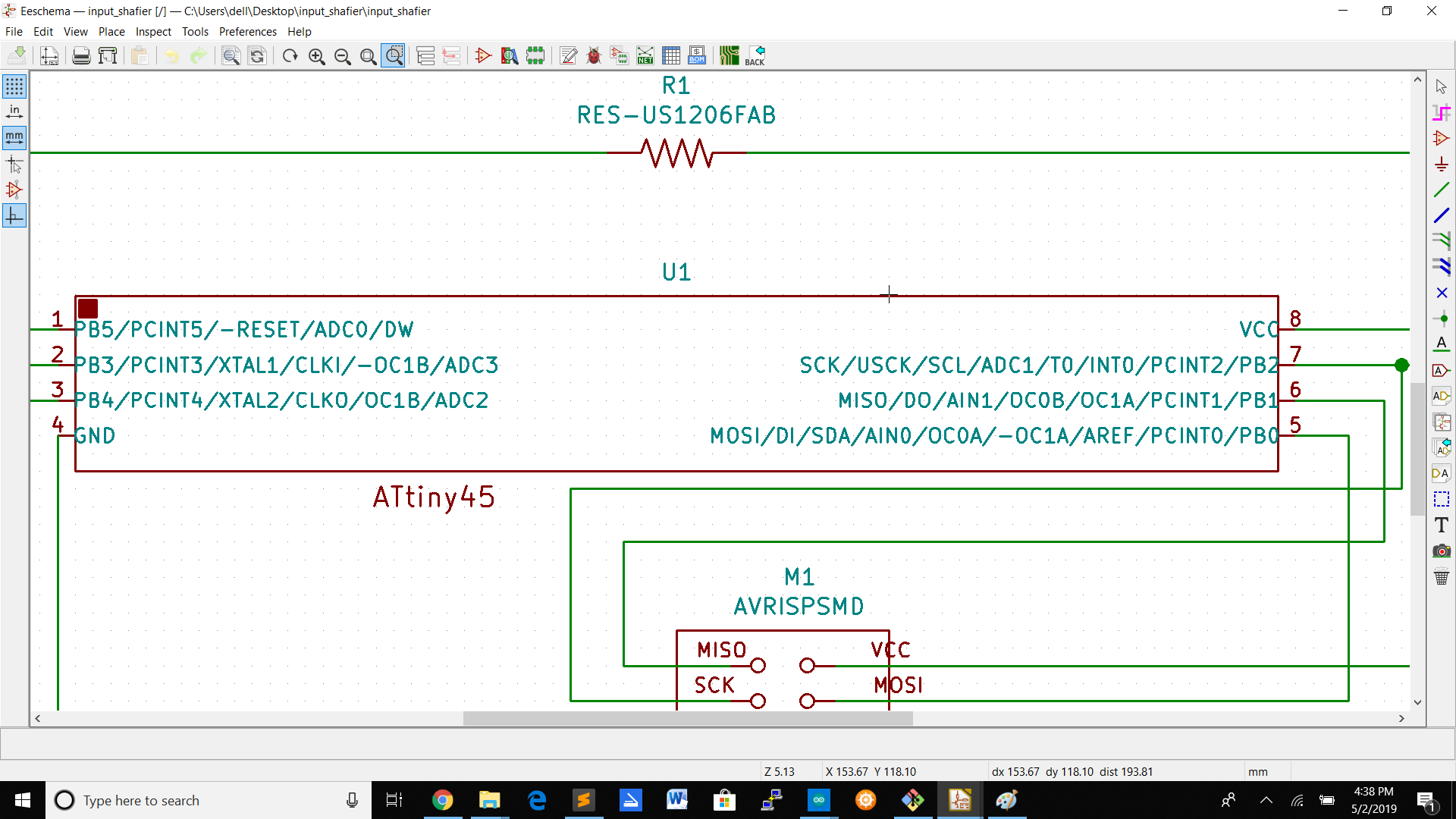
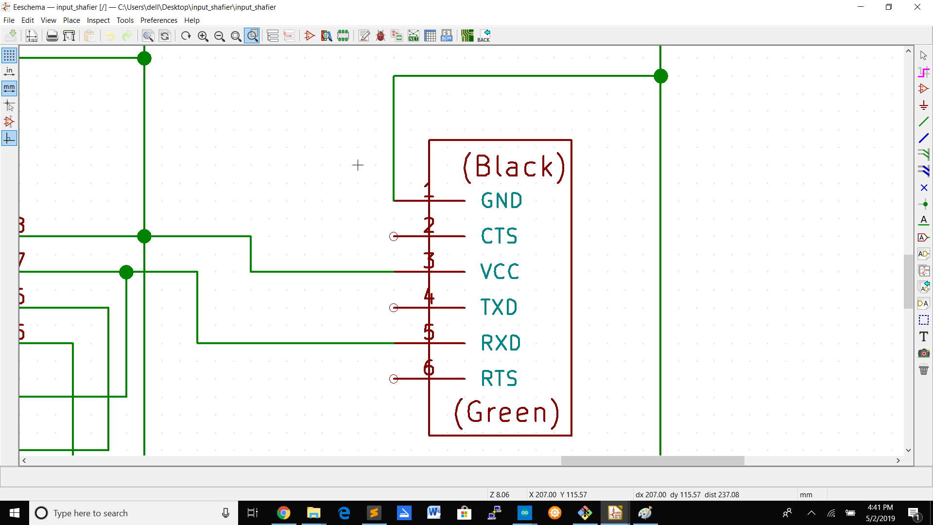
After selecting the components you need ,you have to connect them.To know which component you are going to connect you have to look at the hello button board.The only change is that there is a switch and a 2x2 pinheader extra.To connect the components you have to do that with the wire option on th sidepanel on the right.After wiring the components you have to switch to pcb board schematic.To do that you have to annotate schematic symbols in the top bar and then click on annotate.Then click on update schematic pcb ->Double click on component ->Apply schematics and klik ok->Double click Generate netlist->Save in a folder ->Then tools->Update pcb from schematic ->Update pcb.
KiCad bord design
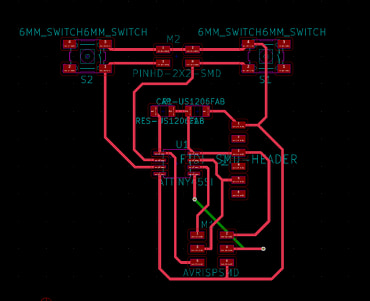
After updating the pcb ,you will get the board design and you will get the components on the board without traces.To connect the components you have to draw the traces.
In this picture you can see that the components are connected by traces.Traces are traces that electrically connect the various connectors and components to each other.To connect the components you can do it with route tracks and you can give routes size(how thick the traces must be and that you can do in setup -> design rules).Also the traces must be straight from component to component and no traces must cross another trace.If that happnes you will get short on your board and you have more chance to get components burned.Your board will not work.
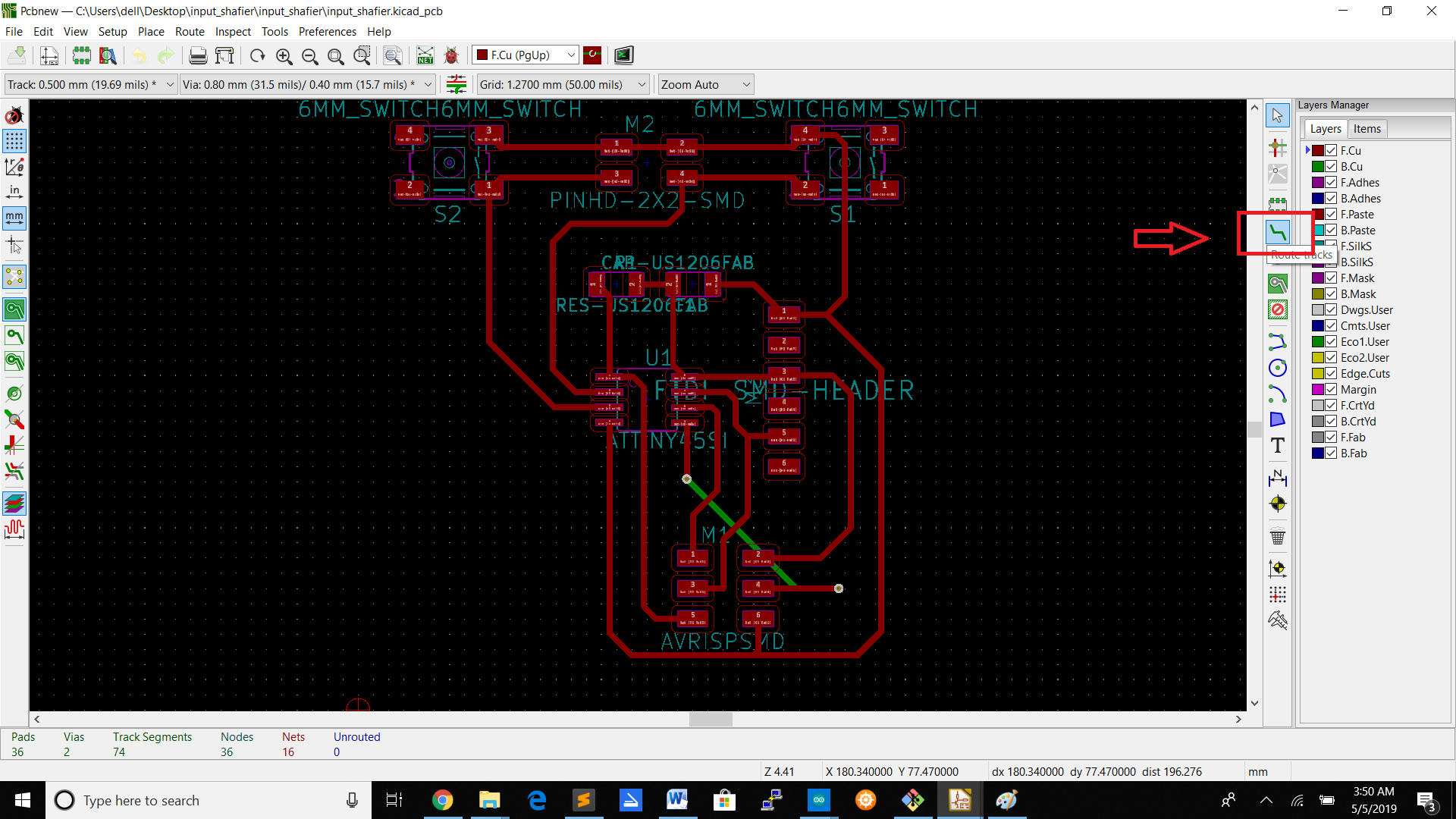
After connecting the components with traces ,you have to double check if you connect the components the right way.When you are connecting the software will also give you a sign where you can connect because you already connected in the schematic design.After connecting the components you have to save your file and to do that you have to :
1.Click on plot on the top bar and select only f.cu(means front cut).
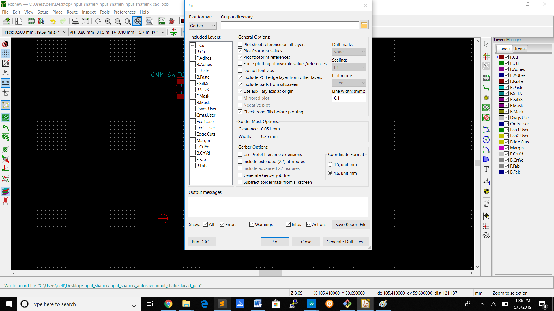
2.Select a output directory where you can save the files.
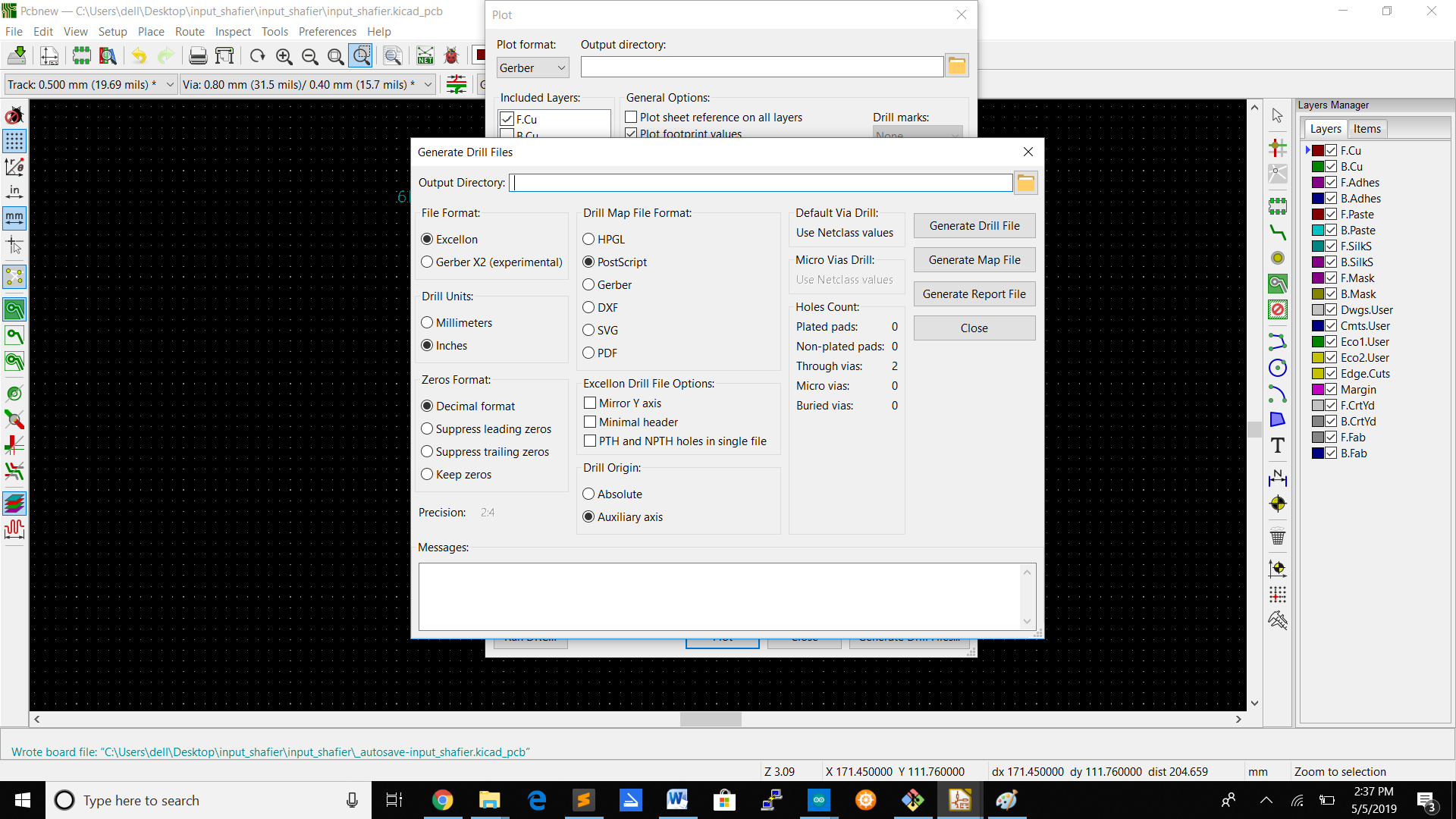
3.Also generate drill files
4.Click on plot
Flatcam
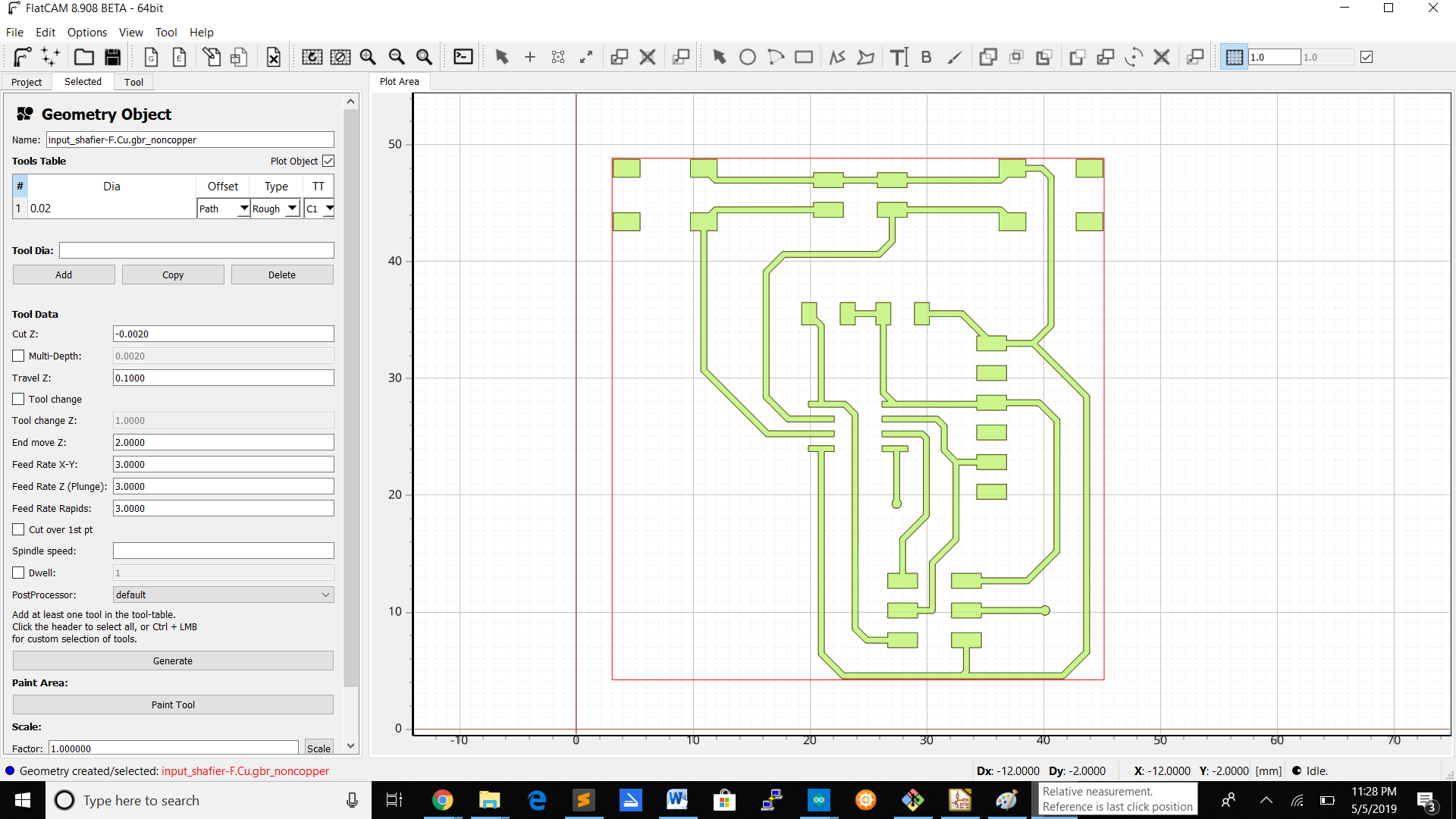
| Tool dia | 0.2 |
| Cut Z | -0.0020 |
| Travel Z | 0.1 |
| End move Z | 2000 |
| Feed rate x-y | 3000 |
| Feed rate Z (plunge) | 3000 |
| Feed rate rapids | 3000 |
After you add the parameters in flatcam ,you have to generate and then select only top copper for milling the traces and save your file in .gbr format to import into Winpc-nc.
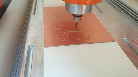
Milling the board
For fasten the board on the mill i used double sided tape.
After fasting your board on to the machine ,you have to set you XY-axis where the board is to set your z-axis.Also have to set the zero point.To do that you have to open winpc-nc ->parameters ->misc. parameters->start/end positions.Check the checkbox of the z-invert coordinates in parameters->import formats.
After doing that you can start the milling of your design in winpc-nc and mill your board.
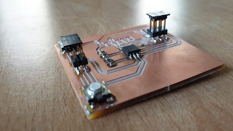
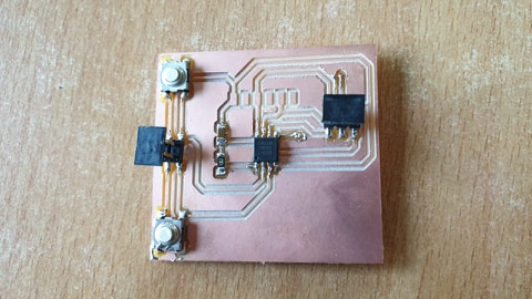
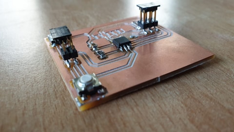
After milling your board i soldered the components on the board.The outcome is :
Programming the board
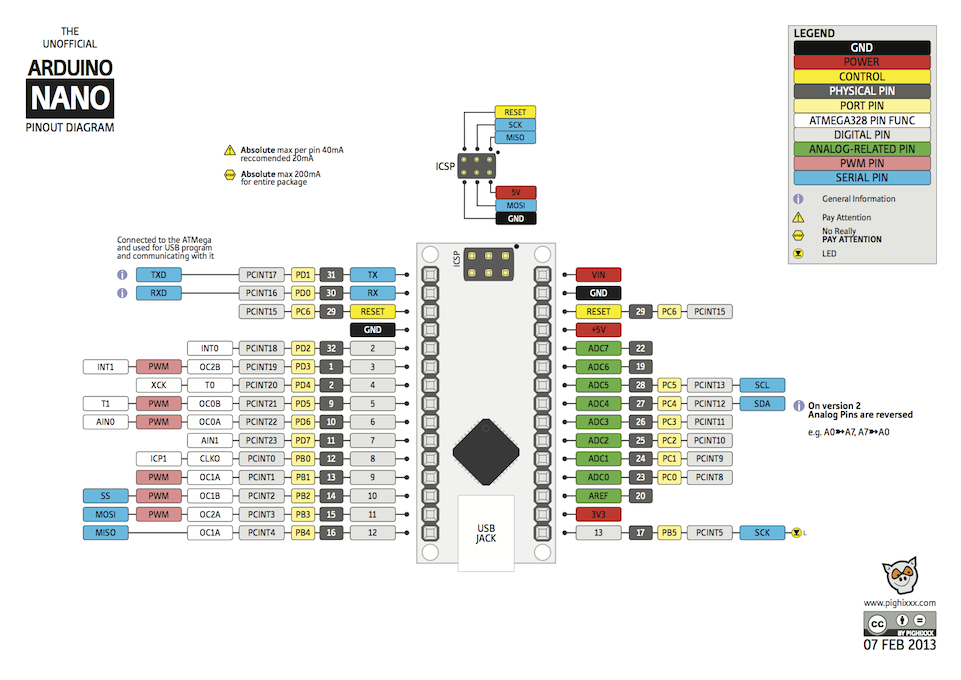
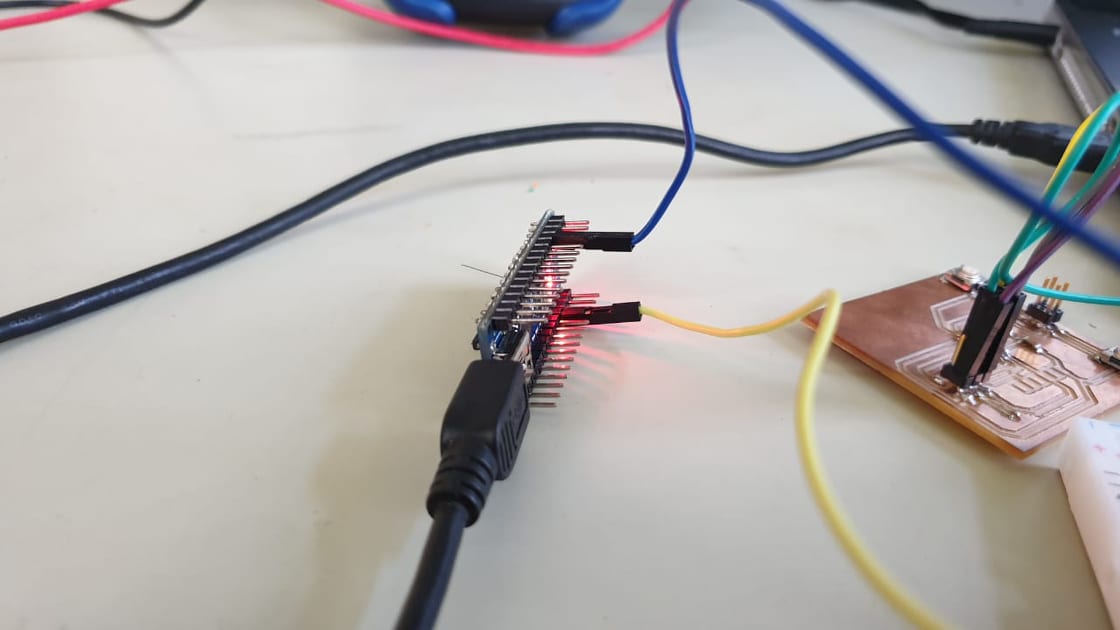
After soldering the components on the board ,you have to program the board.To program the board i used the Arduino nano.
Arduino introduction
Attiny45 introduction
Board Setup
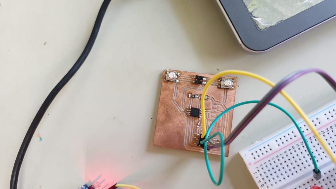
To connect the board i used female to male jumper wires.For programming my code into the board i used the fab isp programmer.
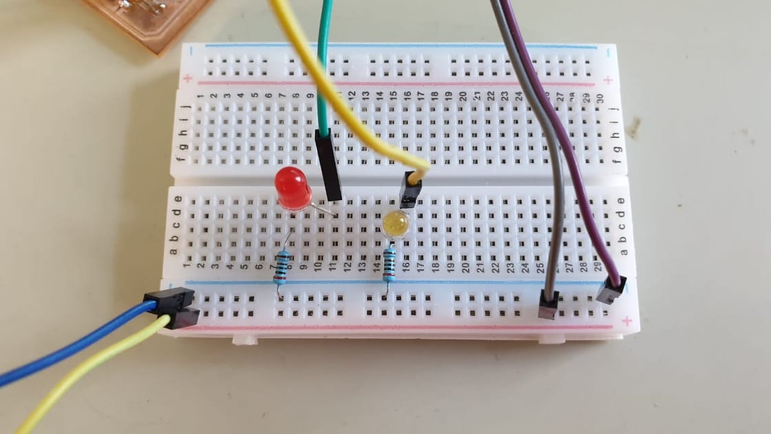
I also used a breadboard to connect some components and tobgive power to components.
For the 5v power i used a arduino nano.The pin voor my buttons are pin 3(button) and pin 4(button1) and for the led is pin 1 and 2.
Arduino code
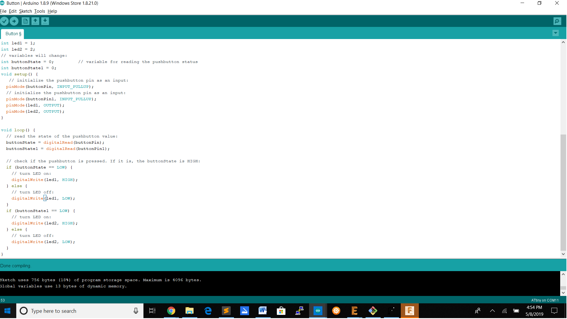
The demo by pushing the buttons.Button 1 is for the red Led and button 2 is for the white Led.
Files
BoardBoard Drill
Board cut
Schematic
Board Design
Button Arduino code